Xilinx and Samsung Launch SmartSSD Computational Storage Drive
by Billy Tallis on November 12, 2020 5:30 PM EST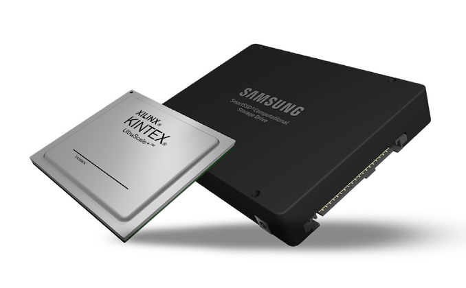
At Samsung's Tech Day 2018 they debuted a collaboration with Xilinx to develop Smart SSDs that would combine storage with FPGA-based compute accelerator capabilities. Their proof of concept prototype combining a Samsung SSD and Xilinx FPGA on a PCIe add-in card has evolved into a 4TB U.2 drive that has completed customer qualification and reached general availability.
The Samsung SmartSSD CSD includes all the guts of one of their high-end PCIe Gen3 enterprise SSDs, plus the second-largest FPGA from Xilinx's Kintex Ultrascale+ (16nm) family and 4GB of DDR4 specifically for the FPGA to use. The SmartSSD CSD uses a portion of the FPGA as a PCIe switch, so the FPGA and SSD each appear to the host system as separate PCIe endpoints and all PCIe traffic going to the SSD is first routed through the FPGA.

In a server equipped with dozens of large and fast SSDs, actually trying to make use of all that stored data can lead to bottlenecks with the CPU's IO bandwidth or compute power. Putting compute resources on each SSD means the compute capacity and bandwidth scales with the number of drives. Classic examples of compute tasks to offload onto storage devices are compression and encryption, but reconfigurable FPGA accelerators can help with a much broader range of tasks.
Xilinx has been building up a library of IP for storage accelerators that customers can use with the SmartSSD CSD, as part of their Vitis libararies of building blocks and and Xilinx Storage Services turnkey solutions. Samsung has worked with Bigstream to implement Apache Spark analytics acceleration. Third party IP that has been developed for Xilinx's Alveo accelerator cards can also be ported to the SmartSSD CSD thanks to the common underlying FPGA platform, so IP like Eideticom's NoLoad CSP are an option.
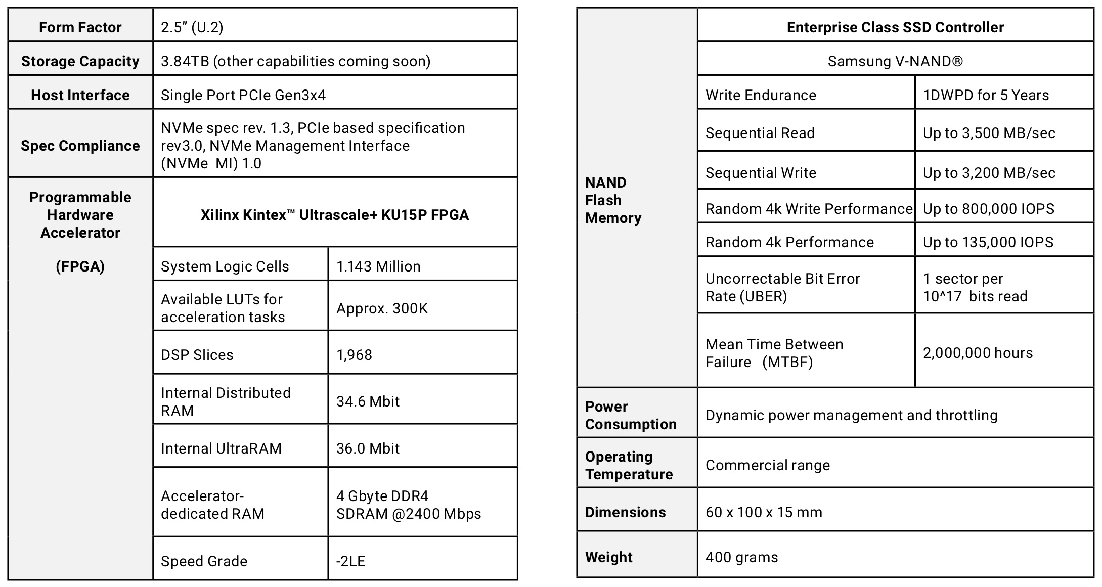
The Samsung SmartSSD CSD is being manufactured by Samsung and sold by Xilinx, initially with 3.84TB capacity but other sizes are planned.


25 Comments
View All Comments
silverj42 - Saturday, November 14, 2020 - link
Thank you - so not available, and the SSD logic takes 800k out of the 1.1M LEs, so this is basically not a real contender for any price above $1000 for me. Too bad, it seemed great at a first glance.Billy Tallis - Saturday, November 14, 2020 - link
LEs aren't the same as LUTs. The FPGA has 523k LUTs, of which about 300k LUTs are available for accelerator IP—roughly equivalent to a KU11P.erinadreno - Saturday, November 14, 2020 - link
Samsung should use ASIC PCIe switch rather than using LUTs on the FPGA. FPGA is for programming, the PCIe switch is a given. But I guess Xilinx just want user to design some DSP only algorithm, which is not totally unreasonable.Billy Tallis - Saturday, November 14, 2020 - link
There aren't a lot of options for small 12-lane PCIe switches. The PLX PEX8714 is 19x19mm and 2.7W, and ASM2812 is 21x21mm. I'm not sure how easy it would be to squeeze one of those into an already crowded U.2 drive.eastcoast_pete - Wednesday, November 18, 2020 - link
It's cool tech for sure, but I am not sure I get why this has to be implemented as an FPGA, and not exactly a small and cheap one, either? Could this be done using, let's say, in software with a decently fast CPU/NPU combo? Why does it have to be implemented as field-programmable hardware?