NVIDIA Announces A100 80GB: Ampere Gets HBM2E Memory Upgrade
by Ryan Smith on November 16, 2020 9:00 AM EST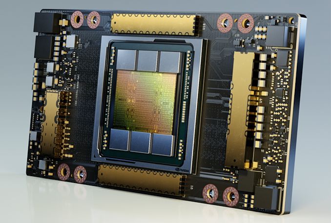
Kicking off a very virtual version of the SC20 supercomputing show, NVIDIA this morning is announcing a new version of their flagship A100 accelerator. Barely launched 6 months ago, NVIDIA is preparing to release an updated version of the GPU-based accelerator with 80 gigabytes of HBM2e memory, doubling the capacity of the initial version of the accelerator. And as an added kick, NVIDIA is dialing up the memory clockspeeds as well, bringing the 80GB version of the A100 to 3.2Gbps/pin, or just over 2TB/second of memory bandwidth in total.
The 80GB version of the A100 will continue to be sold alongside the 40GB version – which NVIDIA is now calling the A100 40GB – and it is being primarily aimed at customers with supersized AI data sets. Which at face value may sound a bit obvious, but with deep learning workloads in particular, memory capacity can be a strongly bounding factor when working with particularly large datasets. So an accelerator that’s large enough to keep an entire model in local memory can potentially be significantly faster than one that has to frequently go off-chip to swap data.
| NVIDIA Accelerator Specification Comparison | |||||
| A100 (80GB) | A100 (40GB) | V100 | |||
| FP32 CUDA Cores | 6912 | 6912 | 5120 | ||
| Boost Clock | 1.41GHz | 1.41GHz | 1530MHz | ||
| Memory Clock | 3.2Gbps HBM2e | 2.4Gbps HBM2 | 1.75Gbps HBM2 | ||
| Memory Bus Width | 5120-bit | 5120-bit | 4096-bit | ||
| Memory Bandwidth | 2.0TB/sec | 1.6TB/sec | 900GB/sec | ||
| VRAM | 80GB | 40GB | 16GB/32GB | ||
| Single Precision | 19.5 TFLOPs | 19.5 TFLOPs | 15.7 TFLOPs | ||
| Double Precision | 9.7 TFLOPs (1/2 FP32 rate) |
9.7 TFLOPs (1/2 FP32 rate) |
7.8 TFLOPs (1/2 FP32 rate) |
||
| INT8 Tensor | 624 TOPs | 624 TOPs | N/A | ||
| FP16 Tensor | 312 TFLOPs | 312 TFLOPs | 125 TFLOPs | ||
| TF32 Tensor | 156 TFLOPs | 156 TFLOPs | N/A | ||
| Interconnect | NVLink 3 12 Links (600GB/sec) |
NVLink 3 12 Links (600GB/sec) |
NVLink 2 6 Links (300GB/sec) |
||
| GPU | GA100 (826mm2) |
GA100 (826mm2) |
GV100 (815mm2) |
||
| Transistor Count | 54.2B | 54.2B | 21.1B | ||
| TDP | 400W | 400W | 300W/350W | ||
| Manufacturing Process | TSMC 7N | TSMC 7N | TSMC 12nm FFN | ||
| Interface | SXM4 | SXM4 | SXM2/SXM3 | ||
| Architecture | Ampere | Ampere | Volta | ||
Diving right into the specs, the only difference between the 40GB and 80GB versions of the A100 will be memory capacity and memory bandwidth. Both models are shipping using a mostly-enabled GA100 GPU with 108 active SMs and a boost clock of 1.41GHz. Similarly, the TDPs between the two models remain unchanged as well. So for pure, on-paper compute throughput, there’s no difference between the accelerators.
Instead, the improvements for the A100 come down to its memory capacity and its greater memory bandwidth. When the original A100 back in May, NVIDIA equipped it with six 8GB stacks of HBM2 memory, with one of those stacks disabled for yield reasons. This left the original A100 with 40GB of memory and just shy of 1.6TB/second of memory bandwidth.
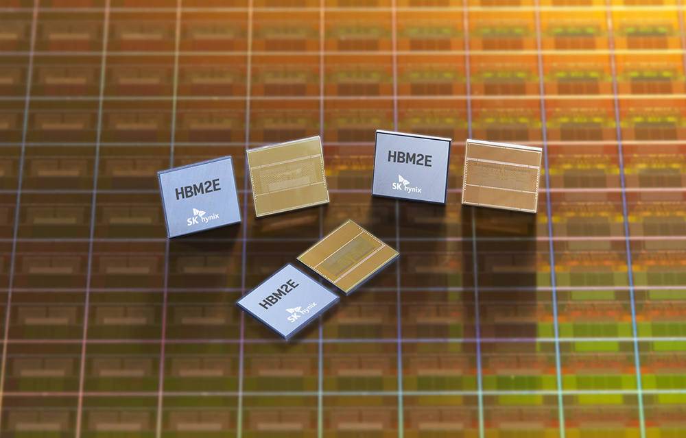
For the newer A100 80GB, NVIDIA is keeping the same configuration of 5-out-of-6 memory stacks enabled, however the memory itself has been replaced with newer HBM2E memory. HBM2E is the informal name given to the most recent update to the HBM2 memory standard, which back in February of this year defined a new maximum memory speed of 3.2Gbps/pin. Coupled with that frequency improvement, manufacturing improvements have also allowed memory manufacturers to double the capacity of the memory, going from 1GB/die to 2GB/die. The net result being that HBM2E offers both greater capacities as well as greater bandwidths, two things which NVIDIA is taking advantage of here.
With 5 active stacks of 16GB, 8-Hi memory, the updated A100 gets a total of 80GB of memory. Which, running at 3.2Gbps/pin, works out to just over 2TB/sec of memory bandwidth for the accelerator, a 25% increase over the 40GB version. This means that not only does the 80GB accelerator offer more local storage, but rare for a larger capacity model, it also offers some extra memory bandwidth to go with it. That means that in memory bandwidth-bound workloads the 80GB version should be faster than the 40GB version even without using its extra memory capacity.
Being able to offer a version of the A100 with more memory bandwidth seems to largely be an artifact of manufacturing rather than something planned by NVIDIA – Samsung and SK Hynix only finally started mass production of HBM2E a bit earlier this year – but none the less it’s sure to be a welcome one.
Otherwise, as mentioned earlier, the additional memory won’t be changing the TDP parameters of the A100. So the A100 remains a 400 Watt part, and nominally, the 80GB version should be a bit more power efficient since it offers more performance inside the same TDP.
Meanwhile, NVIDIA has also confirmed that the greater memory capacity of the 80GB model will also be available to Multi-Instance GPU (MIG) users. The A100 still has a hardware limitation of 7 instances, so equal-sized instances can now have up to 10GB of dedicated memory each.
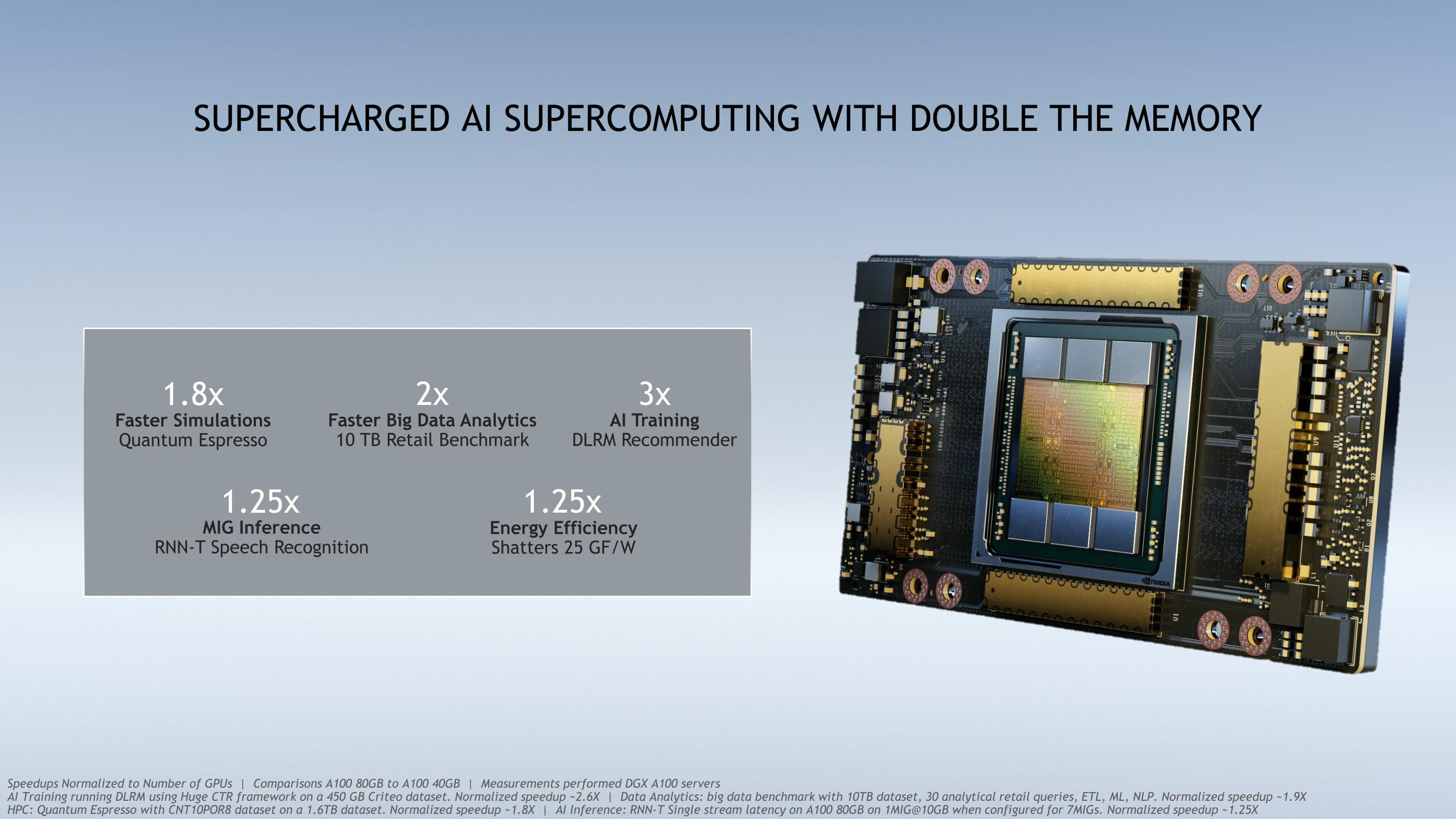
As far as performance is concerned, NVIDIA is throwing out a few numbers comparing the two versions of the A100. It’s actually a bit surprising that they’re talking up the 80GB version quite so much, as NVIDIA is going to continue selling the 40GB version. But with the A100 80GB likely to cost a leg (NVIDIA already bought the Arm), no doubt there’s still a market for both.
Finally, as with the launch of the original A100 earlier this year, NVIDIA’s immediate focus with the A100 80GB is on HGX and DGX configurations. The mezzanine form factor accelerator is designed to be installed in multi-GPU systems, so that is how NVIDIA is selling it: as part of an HGX carrier board with either 4 or 8 of the GPUs installed. For customers that need individual A100s, NVIDIA is continuing to offer the PCIe A100, though not in an 80GB configuration (at least, not yet).
Along with making the A100 80GB available to HGX customers, NVIDIA is also launching some new DGX hardware today as well. At the high-end, they’re offering a version of the DGX A100 with the new accelerators, which they’ll be calling the DGX A100 640GB. This new DGX A100 also features twice as much DRAM and storage as its predecessor, doubling the original in more than one way.

Meanwhile NVIDIA is launching a smaller, workstation version of the DGX A100, which they are calling the DGX Station A100. The successor to the original, Volta-based DGX Station, the DGX Station A100 is essentially half of a DGX A100, with 4 A100 accelerators and a single AMD EPYC processor. NVIDIA’s press pre-briefing didn’t mention total power consumption, but I’ve been told that it runs off of a standard wall socket, far less than the 6.5kW of the DGX A100.
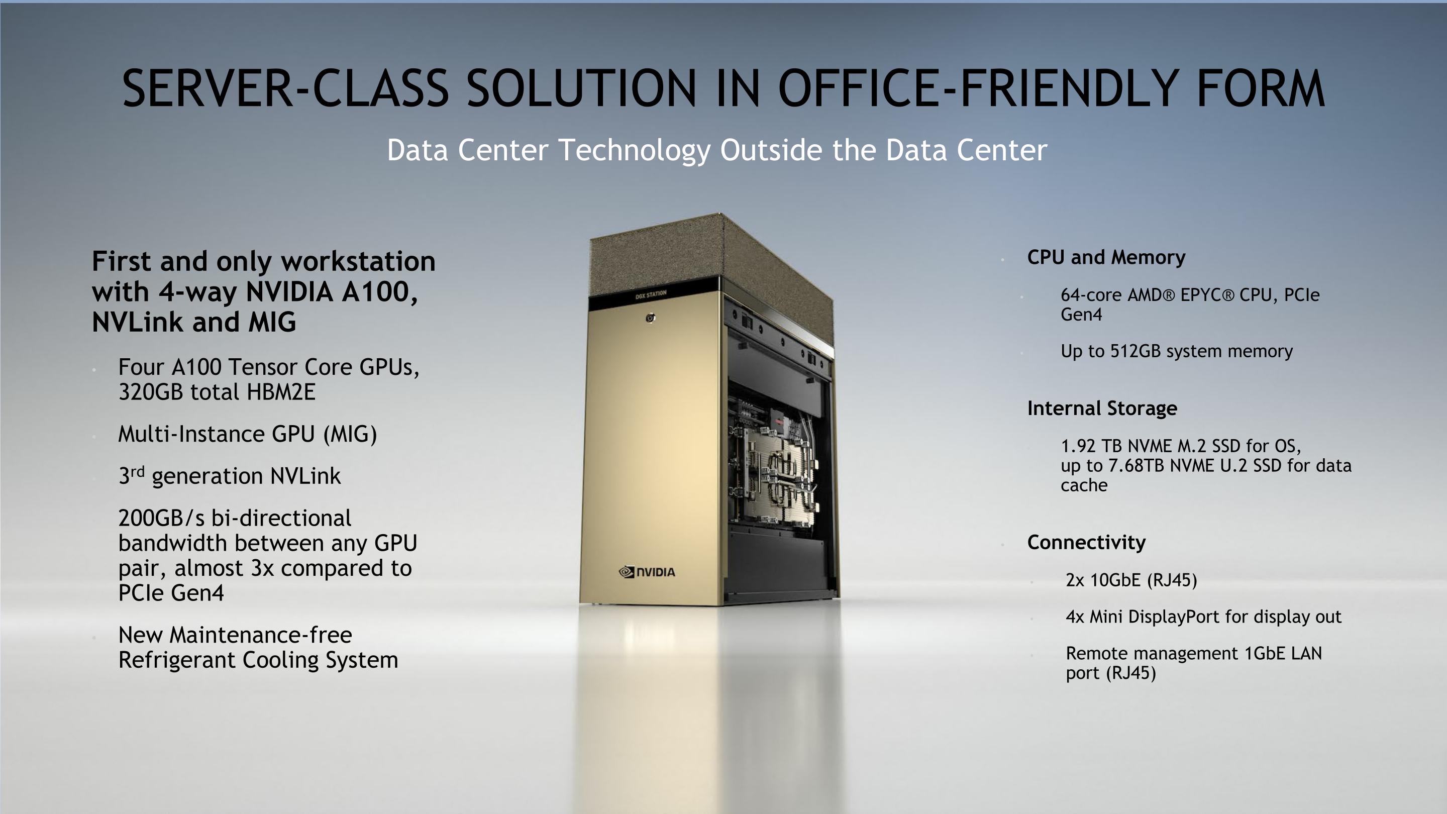
NVIDIA is also noting that the DGX Station uses a refrigerant cooling system, meaning that they are using sub-ambient cooling (unlike the original DGX Station, which was simply water cooled). NVIDIA is promising that despite this, the DGX Station A100 is whisper quiet, so it will be interesting to see how much of that is true given the usual noise issues involved in attaching a compressor to a computer cooling loop.
Both of the new DGX systems as in production now. According to NVIDIA, the systems are already being used for some of their previously-announced supercomputing installations, such as the Cambridge-1 system. Otherwise commercial availability will start in January, with wider availability in February.


29 Comments
View All Comments
Adam7288 - Monday, November 16, 2020 - link
But.....can it run Commander Keen?KusheYemi - Monday, November 16, 2020 - link
Hi Ryan! Why is there no article or write up about the launch of CDNA and the AMD Instinct MI100 accelerator? It is quite a big deal for the HPC market.Cooe - Monday, November 16, 2020 - link
Where's the AMD Instinct M100 (aka "Arcturus") article guys??? Also, I could totally see AMD pulling the exact same move Nvidia pulled here later on.(Aka, releasing a 64GB MI100 w/ HBM2e instead of the 32GB model's HBM2; both doubling capacity AND bumping the memory bandwidth up from 1.28TB/s to 1.6TB/s. And they could potentially even unlock the full 128CU die on top of that [aka +8 more CU's vs standard MI100], to sweeten the deal for the flagship part just that little bit more).
Sychonut - Monday, November 16, 2020 - link
Looking forward to the 500W successor to Ampere. Should be fun getting a second PSU to only power your GPU. The generation after that should be directly plugged into your city's nuclear power plant.Lord of the Bored - Monday, November 16, 2020 - link
But where will we install the second power supply now that cases lack 5.25" bays?You jest, but we used to do exactly that.
TheHughMan - Monday, November 16, 2020 - link
If only we could all get corporate subsidies and tax breaks to afford GPUs and CPUs that perform at maximum threshold.urbanman2004 - Monday, November 16, 2020 - link
Well, I'm sure either option is def above my pay grade, lol. Just wondering how AMD's Instinct MI100 fares against either the 40GB or 80GB version.Kevin G - Monday, November 16, 2020 - link
I wonder when we'll see more fully enabled GA100 chips with the full six stacks of HBM2E enabled. An extra 20% of memory bandwidth and 16 GB of memory would be benefit for many workloads on top of the extra compute units. There is still plenty of performance left in those rare golden samples. I have a feeling nVidia is just stock piling them up for a viable supply as they can't be that common due to yields on a 826 mm^2 die.Santoval - Monday, November 16, 2020 - link
"Both models are shipping using a mostly-enabled GA100 GPU with 108 active SMs..."The Ampere generation is quite confusing; how/why can the "full" GA100 die have 108 SMs, a die size of 826 mm², 6912 CUDA cores and an FP32 performance of "just" 19.5 TFLOPs but the smaller GA102 die of the RTX 3090 has 82 SMs, a die size of 628 mm², *10496* CUDA cores and an astounding FP32 performance of 35.58 TFLOPS?
Is the counter-intuitive difference in cores and FP32 performance simply because the INT (integer) cores were retained on the GA100 but were repurposed as FP32 cores on the GA102? If that's the case is the 3090's FP32 performance somehow "artificially inflated", i.e. it cannot be compared -apples for apples- with the FP32 performance of Turing? Are the integer cores that were "removed" really important for premium consumer cards or are they just used for things like AI (but not games)?
In other words, are AMD's 6800 series cards able to compete (or even slightly surpass) in performance Ampere consumer cards with far more (nominal) FP32 TFLOPs just because the INT cores of the Ampere cards were repurposed or because Navi 2 is a more efficient and effective design?