3nm

Taiwan Semiconductor Manufacturing Co. this week said its revenue for the second quarter 2024 reached $20.82 billion, making it the company's best quarter (at least in dollars) to date. TSMC's high-performance computing (HPC) platform revenue share exceeded 52% for the first time in many years due to demand for AI processors and rebound of the PC market. TSMC earned $20.82 billion USD in revenue for the second quarter of 2024, a 32.8% year-over-year increase and a 10.3% increase from the previous quarter. Perhaps more remarkable, $20.82 billion is a higher result than the company posted Q3 2022 ($20.23 billion), the foundry's best quarter to date. Otherwise, in terms of profitability, TSMC booked $7.59 billion in net income for the quarter, for a gross margin of...
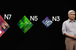
Where are my GAA-FETs? TSMC to Stay with FinFET for 3nm
As we passed that 22nm to 16nm barrier, almost all the major semiconductor fabrication companies on the leading edge transitioned from planar transistors to FinFET transistors. The benefits of...
37 by Dr. Ian Cutress on 8/26/2020
TSMC Details 3nm Process Technology: Full Node Scaling for 2H22 Volume Production
At TSMC’s annual Technology Symposium, the Taiwanese semiconductor manufacturer detailed characteristics of its future 3nm process node as well as laying out a roadmap for 5nm successors in the...
58 by Andrei Frumusanu on 8/24/2020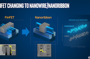
Intel to use Nanowire/Nanoribbon Transistors in Volume ‘in Five Years’
This year, at the international VLSI conference, Intel’s CTO Mike Mayberry gave one of the plenary presentations, which this year was titled ‘The Future of Compute’. Within the presentation...
14 by Dr. Ian Cutress on 6/22/2020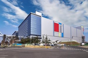
Samsung Starts Mass Production at V1: A Dedicated EUV Fab for 7nm, 6nm, 5nm, 4nm, 3nm Nodes
Samsung Foundry has started mass production of chips using its 6LPP and 7LPP manufacturing processes at its new V1 fab. The new facility employs one of the industry’s first...
30 by Anton Shilov on 2/20/2020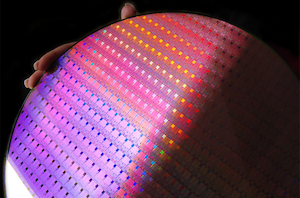
Intel’s Manufacturing Roadmap from 2019 to 2029: Back Porting, 7nm, 5nm, 3nm, 2nm, and 1.4 nm
One of the interesting disclosures here at the IEEE International Electron Devices Meeting (IEDM) has been around new and upcoming process node technologies. Almost every session so far this...
138 by Dr. Ian Cutress on 12/11/2019
TSMC: 3nm EUV Development Progress Going Well, Early Customers Engaged
Development of new fabrication technologies never stops at leading-edge companies such as TSMC. Therefore, it is not surprising to hear the annoucement that development of TSMC’s 3nm node is...
76 by Anton Shilov on 7/23/2019
Synopsys to Accelerate Samsung’s 7nm Ramp with Yield Explorer Platform
Synopsys has announced an acceleration of development on its yield learning platform designed to speed up ramp up of chips made using Samsung Foundry’s 7LPP (7 nm low power...
16 by Anton Shilov on 7/4/2019_carousel.jpg)
Samsung Announces 3nm GAA MBCFET PDK, Version 0.1
So what comes after 7nm, after 6nm, after 5nm, and after 4nm? That's right: 3nm! At Samsung's Foundry Forum event today, Samsung has announced that the first alpha version...
32 by Dr. Ian Cutress on 5/14/2019
Samsung Foundry Updates: 8LPU Added, EUVL on Track for HVM in 2019
Samsung recently hosted its Samsung Foundry Forum 2018 in Japan, where it made several significant foundry announcements. Besides reiterating plans to start high-volume manufacturing (HVM) using extreme ultraviolet lithography...
29 by Anton Shilov on 9/6/2018
GlobalFoundries Gives 7 nm Capacity Update, Mulls Skipping 5 nm
High-ranking executives of GlobalFoundries this month gave several updates concerning future plans of the contract maker of semiconductors. As it appears, in a bid to provide more tangible advantages...
19 by Anton Shilov on 5/31/2018
Samsung Foundry Roadmap: EUV-Based 7LPP for 2018, 3 nm Incoming
Samsung Foundry this week updated its fabrication technology roadmap, introducing a number of changes and announcing the first details about its 3 nm manufacturing process that is several years...
25 by Anton Shilov on 5/24/2018


